New here? Free $20 coupon.


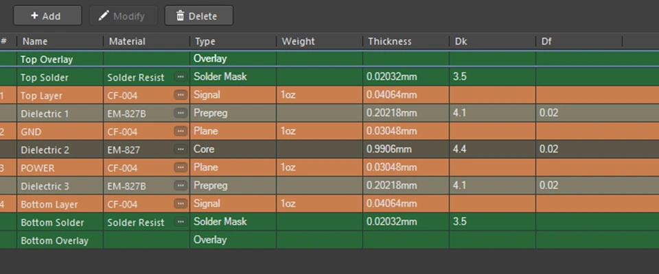
In DWG, customer mentioned layers order only, but didn’t indicate the dielectric thickness between layers and Copper thickness. So, we suggest you follow the stack-up shown on attached file XX. Please confirm.
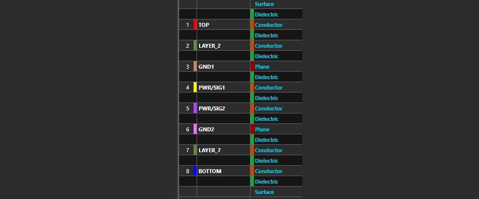
According to the stack-up specified by customer, the overall board thickness will be XXX mil, not the customer nominal requirement of YYY mil. So, we suggest:
A). To follow the stack-up specified by customer and change the overall board thickness to YYYmil+/-10%, OR
B). To modify the stack-up as shown on attached file and control the overall board thickness to be XXX mil per customer requirement.
Please clarify which item (A or B) customer preferred.
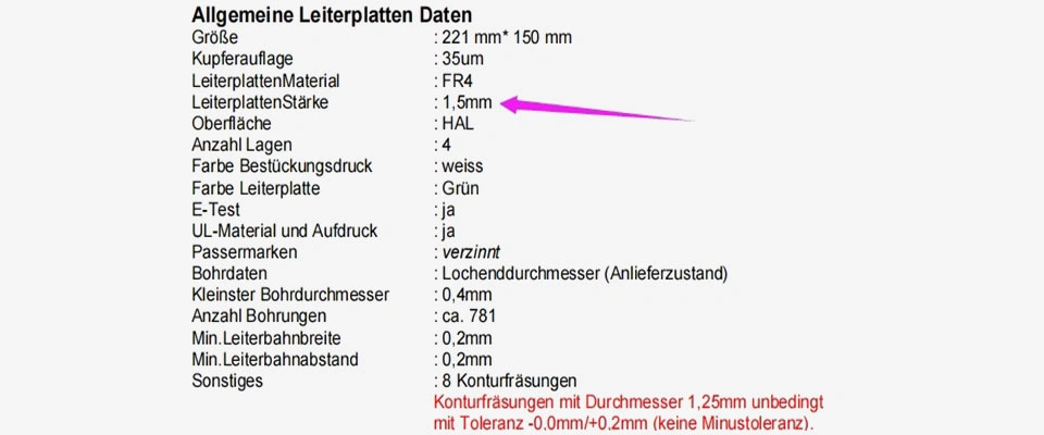
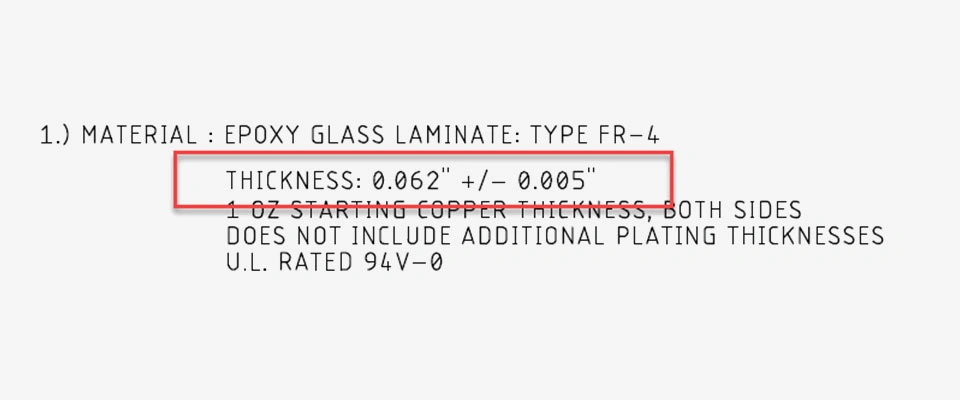
Customer required controlling the finished board thickness to be XXmm+/-%, however, the standard tolerance for board thickness is +/-10%. It’s too tight for us, We can achieve tighter tolerance by ordering non-standard materials, however, it will take a long lead-time and a high price to purchase this special material.
So, we suggest you relax the tolerance from XX% to +/-10%. Please confirm.
According to the stack-up specified by customer, the calculation of impedance can not meet the impedance control requirement, it’s out of the trace width’s tolerance. we suggest to adjust the dielectric thickness as ours, that it can meet both the overall board thickness and impedance control, the stack-up shown on attached file XX, Please confirm
According to Panel DWG, the connection area is far away from unit edge. The tab may be damaged due to unbalancing strength on profiling process. So, we suggest you move the connection area close to Unit edge. Please confirm.
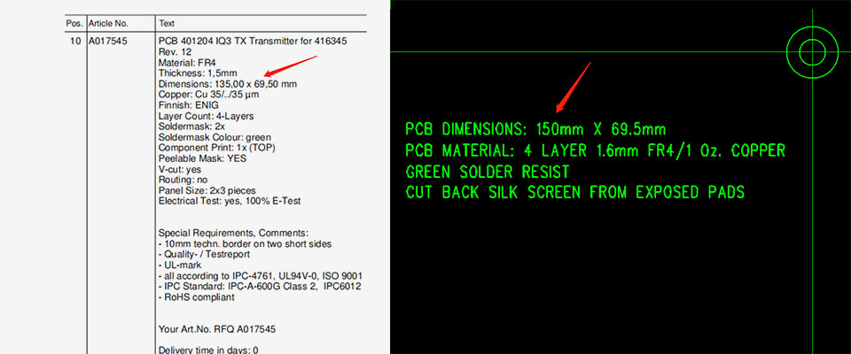
Mismatch was found about a dimension of hole to hole (hole to edge/edge to edge) between CAD/CAM data and DWG:
CAD/CAM DWG
XXX mil YYY mil
We suggest to follow XXX/YYY in CAD/CAM (DWG) to build. Please confirm.
There missed XXX dimension in UNIT/PANEL DWG. After measuring CAD/CAM data, we got these dimensions as attached file. Anyway, we will follow CAD/CAM data to build. Please confirm.
According to panel DWG, the connection area between breakaway holes is 10mil only (less than 15mil), which is so weak that it is very easy to broke off on our process or during delivery. In order to strengthen the connection, we suggest you relax the breakaway hole from XXX mil to DIAYYY mil. Please confirm.
Is this blind hole design for your component bonding purpose? So that copper plating is required on these blind hole surfaces. Please specify and confirm.
Per the breakaway detail, the breakaway hole would be located partially on the copper planes of all layers. We suggest to create a suitable clearance (about 0.50mm larger than the hole size). Please confirm.
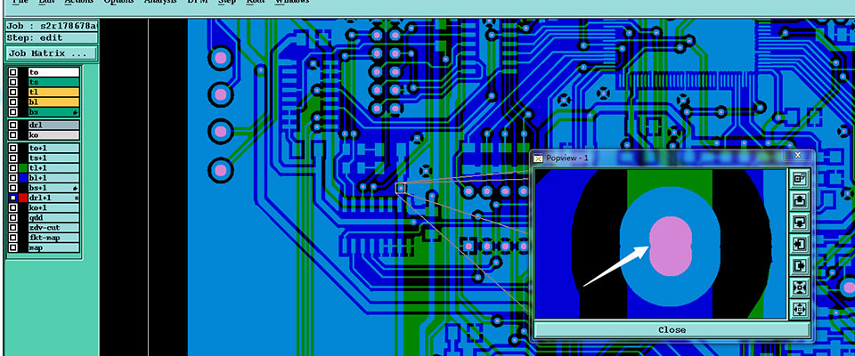
On drill file, three holes (PTH/NPTH, DIA: VVV) are overlapped each other, the distance between two holes is XXX mil. In order to facilitate in production, we suggest you change them as a slot. Please confirm.
Customer required controlling the drill positional tolerance to be +/-X mil, however, the standard tolerance for drill positional accuracy is +/-3mil. Tighter tolerance can be achieved with special processing. In order to facilitate in production, we suggest you relax the tolerance from +/-X mil to +/-3mil. Please confirm.
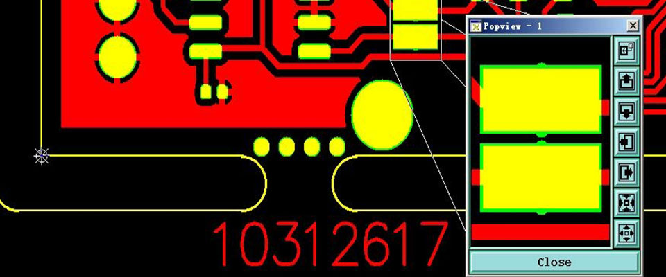
On master A/W, there is no S/M Bridge between neighboring SMT pads. This presents the risk of solder short on assembly process. So, we suggest to add S/M Bridge between them. Please confirm.
According to master A/W, some via hole is plugged with solder mask on one side of the board but has an opening on the other side, then, on hot air leveling, the solder will flow in hole from the side with the opening but can’t flow out of the hole form the side. The result may be a solder ball in hole after HAL. So we suggest:
A). To accept solder balls in these holes, OR:
B). To change S/M plugging side to have a 3mil opening.
Please clarify which item (A or B) customer preferred.
Customer required plugging the via holes of DIA: XXX mil with solder mask. For hole diameters greater than 30mil, we can’t assure that solder mask will fill and plug every hole. We suggest you:
A). Reduce hole size from XXX mil to YYY mil and plugged via hole per master A/W. Please confirm. OR:
B). Change the plugged holes to covered holes. Please confirm.
Please clarify which item (A or B) customer preferred.
Customer required covering the via holes of DIA: XXX with solder mask. For hole diameter smaller than 10mil, because of the misregistration, it is very easy that solder mask flow into hole and block the hole. In order to facilitate in production, we suggest:
A). To change the covered hole to the plugged hole. OR:
B). To add a S/M opening larger than finished hole size by 5mil per side.
Please clarify which item (A or B) customer preferred.
Some legend markings lay on pad fell into hole. If spacing is available, we suggest to move them to suitable place, if not, we will clip the part on pad. Please confirm.
There are some legend markings on solder surface. In order to facilitate in production, we suggest you remove them. Please confirm.
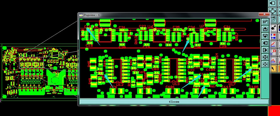
Per master artwork, there are some legends located on the step area (between laminate and copper pattern), which would cause the silkscreen illegible by physical performance.
So we suggest to move or shrink them to suitable area if possible (see jpg file and modified file).
Please confirm.