New here? Free $20 coupon.


| No. | Item | Manufacturing Capabilities | Illustration |
|---|---|---|---|
| 1 | Material | FR-4 (Fiberglass) | Please check below Material List |
| 2 | Number of Layers | 1 Layer, 2 Layers, 4 Layers, 6 Layer, 8 Layers,10 Layers | Standard stackup for multilayer pcbs. |
| 3 | TG Grade | TG130~140, TG150~160, TG170~180 | |
| 4 | Max PCB Size | 1 layer & 2 layers: 1200*300mm or 600*500mmMulti-layers: 600*500mm |  |
| 5 | Min PCB Size | 5mm*5mm | |
| 6 | Board Size Tolerance(Outline) | ±0.2mm(CNC routing)±0.5mm(V-scoring) | |
| 7 | Surface Finish | HASL with lead, HASL lead free, Immersion gold(ENIG), OSP, Hard gold, ENEPIG, Immersion silver (Ag), None | 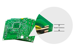 |
| 8 | Board Thickness | 1 Layer/2 Layers: 0.2~2.4mm4 Layers: 0.4~2.4mm6 Layers: 0.8~2.4mm8 Layers: 1.0~2.4mm10 Layers: 1.2~2.4mm Note: Customized PCB thickness and Layer stackup are acceptable. |
|
| 9 | Board Thickness Tolerance | Thickness≥1.0mm: ±10%Thickness<1.0mm: ±0.1mm Note: Normally “+ Tolerance” will occur due to PCB processing steps such as electroless copper, solder mask and other types of finish on the surface. |
|
| 10 | Outer Layer Copper Thickness | 1oz/2oz/3oz(35μm/70μm/105μm) Note: 2ozPCB thickness≥1.2mm,Via size≥0.25mm,Min Track/Spacing≥0.15mm 3ozPCB thickness≥2.0mm,Via size≥0.3mm,Min Track/Spacing≥0.2mm |
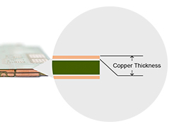 |
| 11 | Inner Layer Copper Thickness | 1oz/1.5oz(35μm/50μm) | |
| 12 | Outer layer Min track/spacing | ≥3mil | 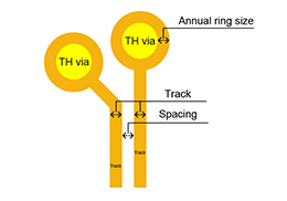 |
| 13 | Inner layer Min track/spacing | ≥4mil | |
| 14 | Annular Ring Size | ≥0.13mm | |
| 15 | Grid Line track/spacing | ≥0.2mm | 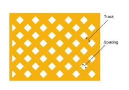 |
| 16 | Coil board Line track/spacing | ≥0.2mm | 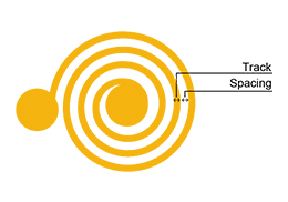 |
| 17 | BGA pad size | ≥0.25mm | 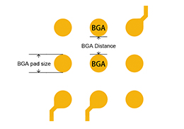 |
| 18 | BGA Distance | ≥0.12mm | |
| 19 | Board Outlines | Track to Outline: ≥0.3mm Trace to V-cut line: ≥0.4mm | 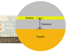 |
| 20 | Finished Hole Size Tolerance | ±0.08mm | 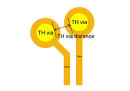 |
| 21 | Finished Hole Diameter(CNC) | 0.2mm~6.3mm 1. PCB Thickness=2.0mm, Minhole size is 0.3mm2. PCB Thickness=2.4mm, Min hole size is 0.4mm3. Copper Thickness=2OZ, Min hole size is 0.25mm4. Copper Thickness=3OZ, Min hole size is 0.3mm |
|
| 22 | TH Via Distance | Same nets: 0.15mmDifferent net: 0.25mm | |
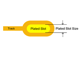
| 23 | Plated Slot Size | ≥0.5mm Note:L:W=2.5: 1 (Should be 2.5:1 or higher. If it is less than this, the holes may be misaligned.) If you can’t draw a long hole in your design, you can draw a continuous round hole and it will be regarded as a long hole. Also, it is okay to draw the oblong hole in Profile Layer instead of Drilling Layer. |
 |
| 24 | Castellated Holes | ≥0.6mm | 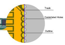 |
| 25 | Non-Plated Holes | ≥0.8mm | 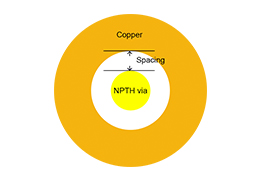 |
| 26 | NPTH to Copper Line | ≥0.2mm | |
| 27 | Soldermask | Green, Red, Yellow, White, Black, Blue, Purple, Matte Green,Matte Black,None | 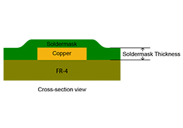 |
| 28 | Soldermask Thickness | 20~30um | |
| 29 | Soldermask Bridge | Green: ≥0.1mmOthers: ≥0.15mm | 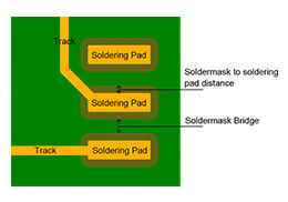 |
| 30 | Soldermask to soldering pad distance | ≥0.05mm | |
| 31 | Silkscreen | White, Black, Yellow, None | 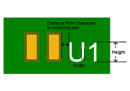 |
| 32 | Minimum Character Width(Legend) | ≥0.15mm Note: Characters of less than 0.15mm wide will be too narrow to be identifiable. |
|
| 33 | Minimum Character Height (Legend) | ≥0.75mm Note: Characters of less than 0.8mm high will be too small to be recognizable. |
|
| 34 | Character Width to Height Ratio (Legend) | 1: 5 (In PCB silkscreen legends processing, 1:5 is the most suitable ratio) | |
| 35 | Silkscreen to Soldering Pad Distance | ≥0.1mm | |
| 36 | V-cut Line | ≥70mm Note:PCB thickness≥0.6mmDetails refer to right side picture |
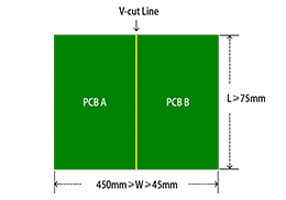 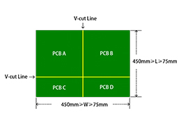 |
| 37 | V-cut Line Distance | ≥3.5mm | 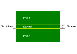 |
| 38 | Distance betwen Board to Board | ≥0.8mm | 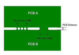 |
| 39 | Stamp-hole Width | ≥2.0mm Note: PCB size and thickness are subject to review by PCBGOGO. |
|
| 40 | Tab-route Width | ≥1.6mm Note: PCB size and thickness are subject to review by PCBGOGO. |
|
| 41 | Edge Rail | ≥3.5mm Note: If choosing panel by PCBGOGO, we will add 5mm edge rails on both sides by default. |
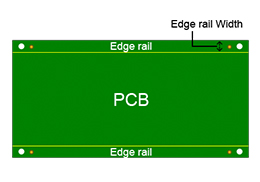 |
| 42 | Gold Finger | Bevelling Angle: 30~45°Depth: ≥1mmLength: 45mm~280mm Note: Board thickness≥1.2mm |
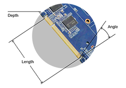 |
| 43 | Special Specification | Impedance controlCustom Layer StackupInterstitial Via Hole(IVH)Via in padVia filled with resinCountersinks/CounterboresCarbon MaskHalogen-FreeZ-axis millingEdge PlatingOthers |