New here? Free $20 coupon.


We offer Kitted and Full Turnkey Assembly service. Whether you supply the parts or we do, our certified assembly technicians can build your quality products with state-of-the-art SMT and Through Hole Equipment.
Surface Mounting(SMT)
Through Hole(THT)
Mixed Technology(SMT+THT)
Single or Double-sided Placement
Hand Soldering
Box Building/Finished Products Assembly
Passive Down to 01005 size
Ball Grid Array(BGA )
Quad Flat Package No-lead(QFN)
Quad Flat Package (QFP)
Small Chip Package(Pitch of 0.3mm)
You provide all the parts including the bare printed circuit boards and electronic components, we assemble your boards using our state of the art automated equipment.
You provide the “hard to find” parts, the “custom” parts, the parts you have in inventory, whatever parts you have! We help procure the rest of the parts, manufacture the PCBs, whatever you don’t provide,then assemble your circuit boards.
We manage the entire process from manufacturing the bare printed circuit boards and all parts through assembly and testing as your application requires.
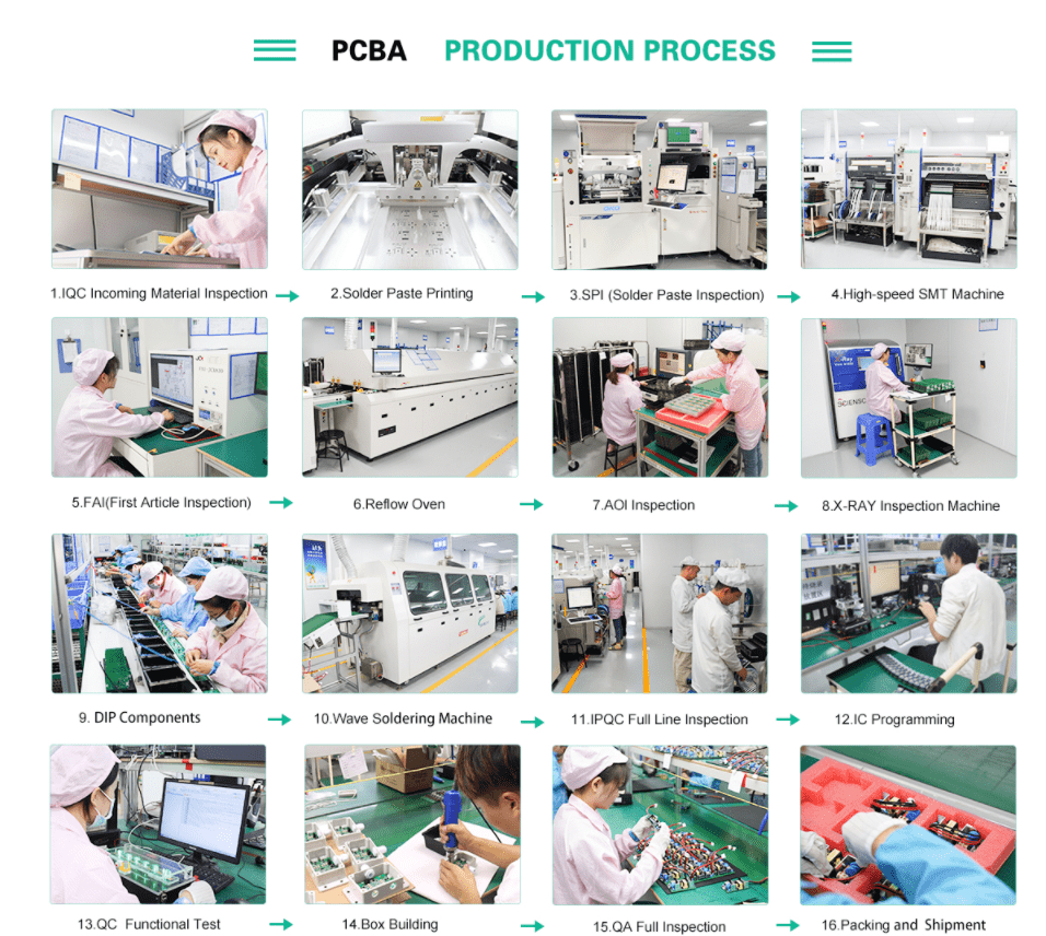
JH PCBA provides one-stop PCB and PCBA manufacturing service, it’s convenient for you to get quoting price and place orders to us.
① Place orders by our online inquiry and ordering system.
② Place orders by sales after confirm orders with sales
Once you order on our platform or by our sales, our pre-review engineers will download your Gerber files and BOM files
① For Gerber files, organize them firstly to check whether necessary files or information are full or some inconsistent PCB parameters or requests described in gerber files and instruction files. View and record into our online s
② For BOM files, organize them firstly to check whether necessary information full or some inconformity such as component part number is not compatible to parameters in description, then check our stock quantity, consult components manufacturer or agent for price, lead time, stock and lot etc information. If some your requested components are out of stock, our purchasing engineers, with rich electronic components knowledge and purchasing experience, will suggest you use same or higher quality alternative components.
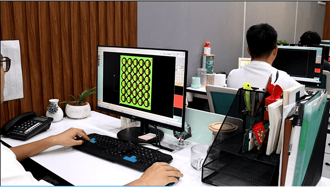
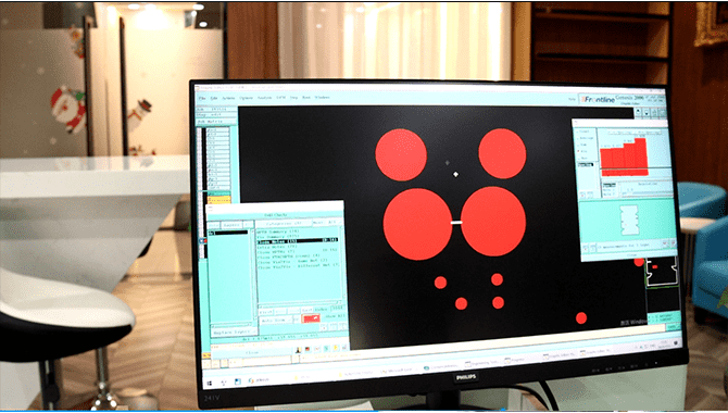
CAM Engineers with more than 5 years, check all pcb specifications and do some optimization in line with manufacturing. Such as to find possible any missing, redundant or potentially problematic features. Any of these issues miss checking or not proper dealing may severely influence the functionality, which leads to PCB and PCBA scrap. For example, one common PCB design flaw is leaving too little spacing between PCB component pads, which result in shorts and other malfunctions.
① DFM Checking can find out unreasonable points of pcb design and do some proper optimization ahead of time, optimize gerber file combing with production capability, is the most important measurement connecting pcb design and real production. DFM Checking can find out problems ahead of time, avoid late serious loss after production already begin without checking, reduce scrap, make production smoothly going ahead, improve one time pass rate.

JH PCBA Verify all incoming materials and handling quality problems before subsequent SMT assembly begins. JH PCBA make sure just buy 100% original and new components from reputable manufacturer or agent, never use faulty or recycle components. Our IQC position will check following issues of incoming materials if they comply with our strict requirements.
•PCB board: Checking appearance: solder mask bubbles, flatness, delamination, dirty, oxidation, copper exposure, board edge burr, hole plugged etc; PCB board silkscreen whether compatible to components part number, polarity etc in BOM
• components part number, brand, parameter description, specifications whether compatible to real components according to BOM list
• shape (deformation, broken pin, oxidation etc), particularly for IC or other complex components
• incoming components standard value, specifications, model number, accuracy, outline dimension whether compatible to design specifications.
• Pin foot numbers and spacing checking: For SIP、 IC、connector、 button、 inductor, IQC will check pin foot numbers, pin spacing according to pcb silkscreen character and pad location, to make sure incoming material correct and conformance.

Machine programming is to setup the various machines such as SMT, AOI, First Article machines etc using Gerber / CAD / BOM/ XY coordinates file which provided by customer to tell machines how to manufacture and inspect PCB.
The first machine to setup in the manufacturing process is the solder paste printer which is designed to apply solder paste using a stencil and squeegees to the appropriate pads on the PCB. Our GKG Gse high-precision, high-stability automatic visual printing machine, can provide the functions required for efficient and precise printing,printing accuracy ±0.025mm.

After solder paste print finish, boards transferred to SPI machine to detect paste print quality by connection rail, such as solder paste volume, area, height, shape, offset, connecting solder, insufficient solder, excess solder tip, solder collapse, variant shape etc. SPI inspection can make sure the solder pad are all with high quality before place components on them. Any solder problem found out, PCB boards need to be cleaned up solder and re-print again.

SMT First Articles means the first one piece board or the first several pieces boards when SMT workshop transfers to new product, workers change shifts, restart after production pause. FAI inspection must be implemented and confirmed without any problem, then subsequent production can be continued, or must to stop to find the fail reasons and adjust machines parameters and implement FAI again, till first articles are qualified.
First Article Inspector(FAI), via compare CAD coordinates, BOM list and first PCBA sample scanning photo datas, to find possible components wrong, missing, polarity reversed etc. Inspection datas are automatically recorded into system, any manual record is not allowed to aviod human errors, which help complex first SMT sample test to be simplified, inspection efficiency to be improved, realize high efficent and high quality SMT first article inspection.

Once the printed PCB has been confirmed to have the correct amount of solder paste applied it moves into the next part of the manufacturing process which is component placement. Each component is picked from its packaging using either a vacuum or gripper nozzle, checked by the vision system and placed in the programming location at high speed.
Our SMT machines are YAMAHA brand YSM10+YSM20R combining group, can place regular and irregular at same time to improve flexible adaptability and high efficiency to various kinds of components. YSM20 placement speed 300,600 solder pads/h, placement accuracy: Chip/QFP/BGA ±0.035m, can meet fast and high-accuracy placement meet. Combined YSM10 muti-functional machine can place components size between 03015~45×45mm, can easily cope with kinds of irregular and relative bigger components.

PCB mounted with components, after soldering reflow oven, can fix components onto PCB by solidifying solder paste. JT lead-free Reflow soldering Oven has 10 temperature zones, can more accurately control temperature rising and dropping process, to make sure good soldering quality. In order to make sure soldering steady quality, our operators will detect oven temperature twice everyday and persistently improve temperature curve to find out the best suitable curve.

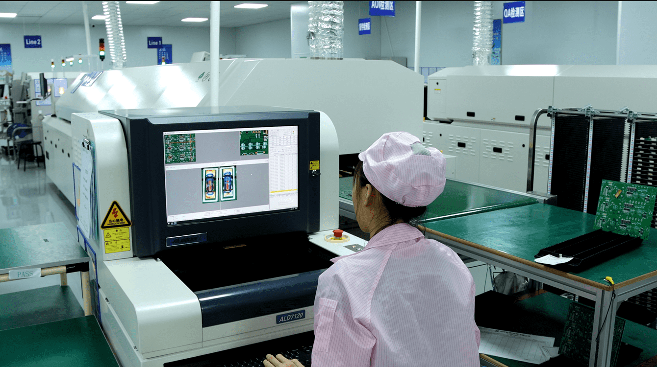
AOI mainly inspect the external solder joints of components.After reflow soldering, PCB board need inspect again to make sure correct soldering and reliable performance. Combining with first article inspection before bulk SMT placement, AOI inspection after reflow soldering can double make sure good quality because after reflow soldering movement, may cause possible unqualified soldering, such as components missing, false soldering, offset, bad components, solder ball, sideward, float, solder bridge, IC pin bend etc soldering defect.
Visual Inspection: Quick check whether have obvious soldering defect in sight.
AOI Inspection: AOI camera automatically scan boards, collect images, compare the scanned soldering points need tested parameters with qualified parameters, via image treatment, find out defects on PCB and mark out so that maintenance staff can proceed rework according to defects places show on display.
X-RAY Inspection: Mainly inspect soldering joints interior defect of BGA、QFN etc high precision components. X-ray has very strong penetrating power, can penetrate the surface of things to see the inner of soldering pads. By using X-ray penetration character, to test and analyse kinds of normal soldering quality problem of electronic components. X-RAY inspection can fully test out the soldering quality of soldering spots, such as short bridge、circuit opening、hole、void、inner bubble and insufficient soldering, and can do quantity analysis too. The biggest characteristic of x-ray is can test out the soldering defect under such BGA encapsulation components, such as bridge connection, short bridge, soldering ball missing, soldering ball offset, insufficient soldering, void, fuzzy edge of soldering ball and soldering pots etc inner quality problem.

After SMT Assembly, semi-finished PCB need THT Assembly to assemble components with pins into PCB, then functional inspection and packing to ship out.
THT First Article Making: IPQC will make a THT First Article by hand according components polarity and components location indicates which indicating the components location on PCB board. Another IPCQ will check the THT First Article and make sure they are qualified.

THT Assembly: THT Assembly production line workers will finish following prototype or volume orders according to THT First Article made by IPQC and work instruction. At this stage, JH PCBA will choose soldering finished by hand or Wave Soldering machine according quantity.

Prototype Soldering: Normally quantity<50pcs, workers will solder these small quantity semi-finished boards by hand.
Volume Soldering: More quantity orders, in order to improve efficiency and quality steady, volume orders will be finished by Wave Soldering machine. Wave soldering is to let PCB soldering side immerse into high temperature liquid tin directly to realize soldering. PCB plugged with components laid on transfer chain, by specific angle and certain immerse depth, go though by immersing in soldering wave peak to realize soldering engineering. Wave Soldering operator are requested every 2h record tin oven temperature, preheat temperature, conveyor speed and angle, soldering flux proportion etc technical parameters, and check 10pcs PCB every hour and record soldering quality. These data can provide original record for process quality control.

Programme Burning: Load the original program into the computer after compiling, and let the computer execute the program you wrote.
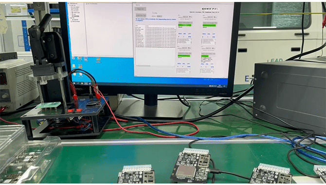
Different product have different test request and method. Customer provide test software,operation directive(test process) and technology instruction, then we will prepare different test fixture and equipment. QA will finish last test to make sure PCBA specifications comply with designer’ requests.
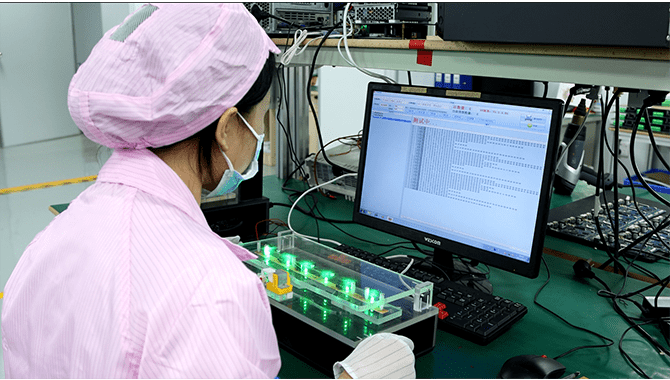
Functional test we can do: ICT,FCT, Aging,durability test etc
16, Washing and Drying
Suffice it to say, the manufacturing process can be a filthy one. Soldering paste leaves behind some amount of flux, while human handling can transfer oils and dirt from fingers and clothing to the surface of the board. Once all is said and done, the results can look a little dingy, which is both an aesthetic and a practical issue.
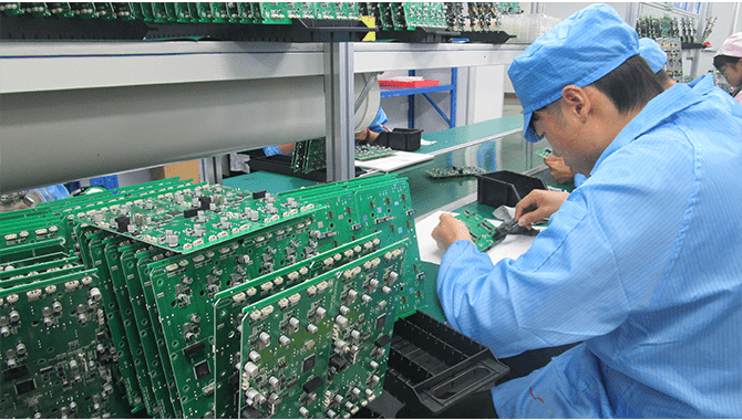
Functional test we can do: ICT,FCT, Aging,durability test etc
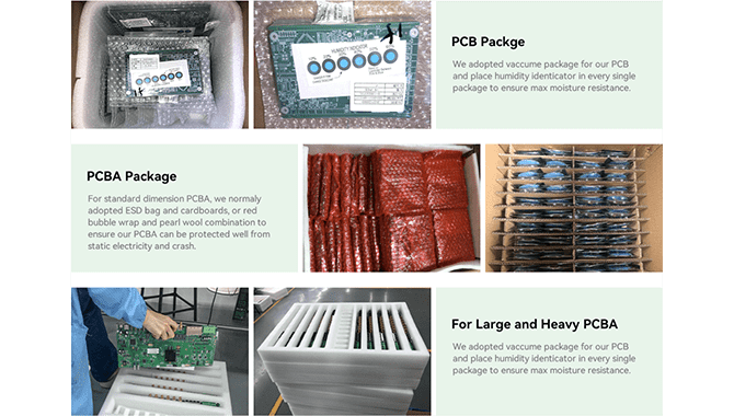
All assembled boards are packaged (can request in anti-static packaging) and shipped DHL,FedEx,UPS,EMS,and so on. Any unused components are returned in accordance with customer instructions. Additionally, customers are notified via email when their packages ships.
Under some possible harsh environment occasions such as Chemical, Vibration, heavy dust, salt-spray, moisture, high temperature etc, need PCBA boards to resist oxidization, corrosion, softening, deformation, getting mouldy and so on bad hurt, so to coat a film of conformal coating is to provide effective protection of PCBA boards from these bad environment destroy, mainly provide various types of protection such as moisture resitant, salt-spray resistant, anti-oxidation, anti-static etc.


