PCBA Testing
The Key to Guarantee PCB functional by SMT Test
PCBA SMT processing is very complicated and includes multiple important processes, such as PCB board manufacturing process, component procurement and inspection, SMT assembly, DIP, and PCBA testing. Among them, PCBA testing is the most critical quality control step in the entire PCBA processing process. The testing determines the final performance of the product. 
Our strengths in PCBA Testing

Visual inspection: general quality check.

FAI: full quality check applied to the first PCB to pass through all stages of production.

X-ray Inspection: checks for BGAs, QFN and bare circuit boards.

AOI Testing: checks for solder paste, 0201 components, missing components and polarity.

3D AOI Testing: checks for missing and misplaced SMT components in three dimensions.

3D SPI Testing: measures the precise volume of solder paste for SMT assembly.

ICT (In-Circuit Test)

Functional test (Following your test procedures)
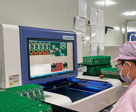
AOI
Automatic Optical Inspection
We use AOI to check the inner layers of multilayer PCB. This inspection is much more reliable and repeatable than manual visual inspection and it will guarantees the high reliability of multilayer circuit boards. AOI visually scans the surface of the PCB. The circuit board is lit by several light sources and observed by a scanner or by a number of high definition cameras. This enables the monitoring of all areas of the printed circuit board. AOI for a bare PCB board inspection will detect the features include:

• Line width violations

• Spacing violations

• Excess copper

• Missing pads

• Cut traces or pads

• Hole breakage
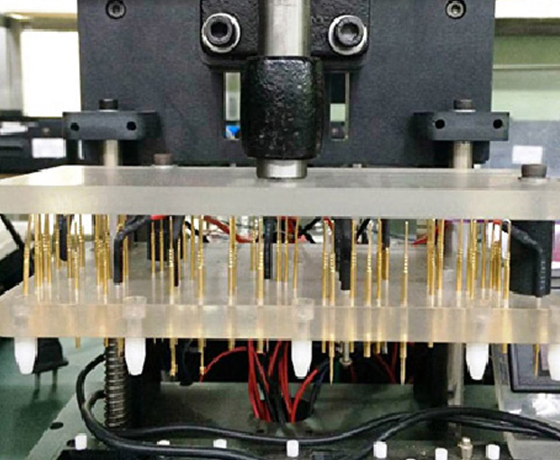
ICT Testing
ICT Performs Comprehensive Testing
PCB In-Circuit Test (ICT) is a technique that uses probes to test the functionality of an assembled PCB. Perform this ICT test to check for shorts or open circuits in assembled electronic circuits. This technique can also help determine the functionality of a PCB by validating factors such as current, voltage, resistance, temperature, etc. by validating the calculated design values. It ensures that the functional values of these factors match the calculated factors to ensure proper functionality. ICT provides OEM customer such benefits as:

• Although a costly fixture is required, ICT covers 100% testing so that all power and ground shorts are detected.

• ICT testing does power up testing and eliminates customer debug needs to almost ZERO.

• ICT does not take a very long time to perform, for example if flying probe takes 20 minutes or so, ICT for the same time might take a minute or so.

• Checks and detects shorts, opens, missing components, wrong value components, wrong polarities, defective components and current leakages in the circuitry.

• Highly reliable and comprehensive test catching all manufacturing defects, design faults, and flaws.

• Testing platform is available in Windows as well as UNIX, thus making it slightly universal for most testing needs.

• Test development interface and operating environment is based on standards for an open system with fast integration into an OEM customer’s existing processes.

• ICT is the most tedious, cumbersome, and expensive type of testing. However, ICT is ideal for mature products requiring volume production. It runs the power signal to check voltage levels and resistance measurements at different nodes of the board. ICT is excellent at detecting parametric failures, design related faults and component failures.
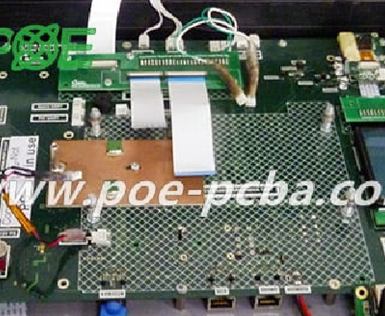
Functional Testing
A Final Manufacturing Step
PCB functional testing is an assembly-level test performed after manufacturing. This test is performed on the PCB to ensure that it functions within the calculated specifications. It tests the presence of components on the PCB, the precise location of the components and their function. There are different types of functional tests for PCBs, all of which are designated for different purposes. The list of various functional tests is as follows

• X-ray inspection/testing

• Microsection Test

• contamination test

• Solderability Test

• Time Domain Reflectometer Test (TDR)

• peel test
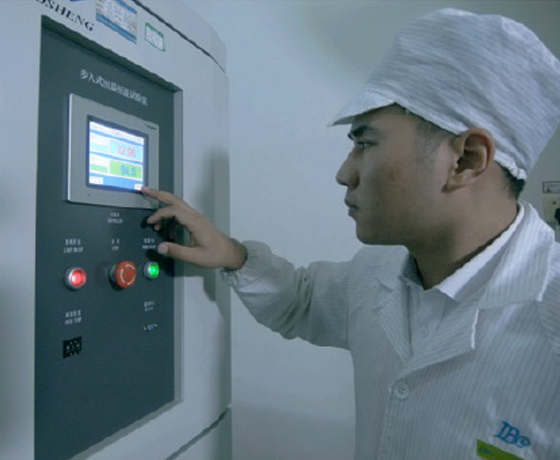
Our testing engineer will preview your requirements such as test scope and test instruction, design the test jig if necessary, set up the instruments, and prepare the test report form and design testing workflow.
Aging test
An Application Specific Integrated Circuit (ASIC) is an integrated circuit specially designed for a specific application, and testing these circuits on a printed circuit board becomes a very critical and complex task. This is where burn-in testing comes into play.
ASIC reliability is checked by performing burn-in testing techniques. This test method is typically performed at a temperature of 125°C (257°F). Tests are performed when power and electrical signals are applied to these specialized ICs.
Basically, this technique is performed before the different components are used. In this testing method, components are stress tested. This helps ensure component and PCB reliability. 
During burn-in testing, ICs placed on the board are put under enormous stress. This helps identify defects and failures. These boards are able to withstand high temperatures during testing. During this process, the temperature remains as high as 257°F (125°C). Again, during this process, the boards are placed in an aging oven. Provide the necessary voltage for the sample to be tested. After completing this stress test, the samples will be screened. This helps make sure they pass the oven test.