New here? Free $20 coupon.


JH PCBA is one of the world’s leading manufacturers of printed circuit boards. Since 2009, JH PCBA has been producing and supplying heavy copper PCB and designs to the world with its excellent quality and reasonable price. With years of industry experience as China heavy copper PCB manufacturer, it has built up a good reputation for its excellent quality and timely delivery.
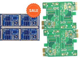
Heavy copper PCB is a circuit board with a copper thickness that is ≥ 3oz per sq. ft in its outer and inner layers. What makes a circuit board classified as a heavy copper PCB is its thicker plating. During the production of heavy copper PCB, copper thickness is enhanced through plated holes and sidewalls.

•Improved thermal performance: Heavy copper PCB can withstand repeated thermal cycles during manufacturing and assembly processes.
• Increased current carrying capacity: Heavy copper PCB offer better electrical conductivity and can handle higher current loads. Increasing the copper trace width can enhance the current carrying capacity, and thicker copper traces can handle even larger current loads.
• Increased mechanical strength: Heavy copper PCB enhance mechanical strength at connectors and plated-through holes, ensuring the board’s structural integrity and making the electrical system more robust and resistant to voltage.
• Excellent dissipation factor: Heavy copper PCB are highly suitable for large power-loss components. These PCB can prevent electrical systems from overheating and effectively dissipate heat.
• Good conductor: Heavy copper PCB are good conductors, making them useful in the production of electronic products. They help to connect various boards together, which can transmit currents.
• Military: Weapons control, radar, and monitoring systems.
• Automotive industries: Rail track system and signal transmission system.
• Power distribution: Excitation systems for power regulators, power grid switching systems, high power rectifiers, and overload relays.
• Transportation: Power converters for railway systems, power line monitors, traction converters.
• Industrial controls: Safety and signal systems, welding equipment, protection relays, surge protectors.
• Renewable Systems: Power converters, energy storage, power grid back-up, hydroelectric power plants control panels.


From $5/10pcsBuild
Time:24 hours


From $5/10pcsBuild
Time:24 hours

From $5/10pcsBuild
Time:24 hours

From $5/10pcsBuild
Time:24 hours

From $5/10pcsBuild
Time:24 hours

From $5/10pcsBuild
Time:24 hours

From $5/10pcsBuild
Time:24 hours

From $5/10pcsBuild
Time:24 hours